Despite the simplicity of this program, I am often asked to write an article on it. But I had no time for everything. Therefore, he took on the role of Captain Obvious Sailanser. Having completed this titanic work. I just corrected it and added some details here and there.
Everyone has probably known for a long time a program for making printed circuit boards called Sprint-Layout, at the moment the latest version is proudly called 5.0
The program itself is very simple and does not require much time to master, but allows you to make boards of fairly high quality.
As I said, the program itself is quite simple, but it has many buttons and menus to help us in our work. Therefore, we will divide our lesson in drawing a board into several parts.
In the first part, we will get acquainted with the program and find out where and what is hidden in it. In the second part, we will draw a simple board that will contain, for example, a couple of microcircuits in DIP packages (and we will make these microcircuits from scratch), several resistors and capacitors, and we will also look at such an interesting feature of the program as Macro creator and use it to make a microcircuit package, for example TQFP-32.
I will also show you how to draw a board from a picture or photograph.
Part 1: What and where we hide and how it helps us in drawing a printed circuit board.
After we found the program, downloaded it, unpacked it from the archive and launched it, we see this window.
First, let's see what's hidden behind the File inscription.
We click on this inscription, and immediately we have a drop-down menu.
 |
- New,Open,Save,Save as, Printer settings..., Seal…, Exit Everything is clear with this brethren. This is not the first day we’ve been sitting in Windows.
- Save as macro... This option allows us to save a selected fragment of a diagram or other parts as a macro, which has the .lmk extension, so as not to repeat the steps to create them again in the future.
- Autosave.. In this option, you can configure autosaving of our files with the .bak extension and set the required interval in minutes.
- Export In this option, we can export to one of the formats, i.e. save our scarf as a picture, as a gerbera file for further transfer to production, save as an Excellon drilling file, and also save as contour files for subsequent creation of a scarf using a CNC machine. Usually useful in preparation for factory production.
- Directories... In this option we can configure parameters for working with the program, such as keyboard shortcuts for file locations, macros, layer colors, etc., etc.
Let's move on to the next item: Editor

The next item we have is Action

Next on our list is Options.
So, the first point is to set up the basic parameters. We can specify the length units in our case mm, specify the color of the hole in the pad, in our case it coincides with the background color and will be black; if later our background is red, then the color of the hole in the pad will also be red. You can also just select the hole color as white, and it will be white no matter what the background is.
The second item we have is Virtual nodes and routes. This item, if it is checked, gives a very interesting property in the program, it places several virtual nodes on the conductor on which we draw.
And the program will automatically add several more virtual nodes in the areas between the real nodes, and we have the opportunity to further edit our track. This can be very convenient when you have to drag, for example, a third track between two already laid ones.
Mirror macros and text on the reverse side
If this item is activated, then when inserting text or a macro onto a layer, the program itself will look at whether it is mirrored or not so that later the details or inscriptions have the correct display on our finished board.
The next item we have is Board Map, this item has one interesting trick: if it is activated, then a small window appears on the left side of our program.
 |
It’s like a smaller copy of our scarf; it’s up to everyone to decide whether to include it or not; it’s up to me personally. Fans of the RTS genre will also appreciate it :)
Pop-up windows are basically all sorts of hints in the program - obviously.
Limit font height (min 0.15mm)
This is the checkbox that many beginners and not only users of this program are looking for; if it is checked, then when we make inscriptions on the board or on elements, we cannot make the size of the letters less than 1.5 mm. So if you need to put text somewhere smaller than 1.5 mm, I recommend removing it. But when sending it to production, this must be taken into account. Not everywhere they can print silkscreens of such low resolution.
Let's go further and see another interesting point, namely Ctrl+ mouse to remember parameters of selected objects, if this item is activated, then one interesting thing appears. For example, we drew two contact pads and laid a track between them, say 0.6 mm wide, then we did something else and something else and in the end we simply forgot what the width of this track was. Of course, you can just click on it and in the track width setting we will see its width,
here, instead of 0.55, our width will become 0.60, but then adjusting the slider to the right of the number in order to adjust the width to 0.6 is lazy, but if we click on the same track with the Ctrl button held down, then our value is 0, 6 will immediately be remembered in this window and a new path, we will draw with a thickness of 0.6 mm.
Using increments of 0.3937 instead of 0.4.
The translation is of course very clumsy in the original, this item is written like this: HPGL-Skalierung mit Faktor 0.3937 statt 0.4 in general, this item is responsible for creating an HPGL file for subsequent transfer to a coordinate machine, and indicates whether to use one decimal place or, depending on the machine, use four characters after the comma.
We are done with the first point and now let’s move on to the second point of our window, it’s called Colors and let’s see what’s hiding there.
There is nothing special here either, we just indicate the paths where and what we have, this setting takes place if we install the program from a distribution downloaded from the official website, but since the program works great for us without any installation, then we simply don’t have to change anything and move on.
Here, too, everything is quite simple and we simply indicate the number by how long the program can roll back changes for us, if something was messed up when drawing our board, I set the maximum number to 50.
Let's move on to the next point, and it's called I max they show movies in 3D format
In it we see keyboard shortcuts for certain operations and if there is anything we can change them, although I didn’t really bother with this and left everything as it is by default.
We are done with the Settings item and let's look at the rest of the options in the drop-down menu Options
Properties
If we select this item, a window will open on the right side of the program
Which will allow us to control our drawn scarf, set restriction gaps, etc. An extremely convenient and extremely necessary thing. Especially when sending boards to production, and even in handicraft conditions it comes in handy. The point is. For example, we set a minimum gap of 0.3mm and a minimum track of no less than 0.2mm, and during the DRC check the program will find all the places where these standards are not met. And if they are not fulfilled, then there may be mistakes in the manufacture of the board. For example, the tracks will stick together or some other problem. There is also a check of hole diameters and other geometric parameters.
Library
When you select this item, we will see another window on the right side of the program.
A very interesting point: it allows you to put a picture as a background on our table in the program where we draw a scarf. I won’t describe it in detail yet, but I’ll come back to it.
Metallization
When selecting this option, the program fills the entire free area with copper, but at the same time leaves gaps around the drawn conductors.
 |
These gaps can sometimes be very useful to us, and with this approach the board turns out more beautiful and more aesthetically pleasing. I’ll also go into more detail about adjusting the width of the gap when we draw the board.
Whole fee
We select this option, the screen will zoom out, and we will see our entire scarf.
All components
Similar to the top point, but with the only difference that it will reduce the scale depending on how many components are scattered across our scarf.
All selected
This item will adjust the screen size up or down depending on what components are currently selected.
Previous scale
Return to the previous scale, everything is simple here.
Refresh Image
A simple option simply updates the image on our screen. Useful if there are any visual artifacts on the screen. Sometimes there is a glitch like this. Especially when copy-pasting large pieces of the circuit.
About the project…
If you select this option, you can write something about the project itself, and then remember, especially after yesterday, that I drew there, it looks like this.
Here we see that we have to drill 56 holes and we need to adjust five of them so that the internal point on the contact pad is 0.6 mm.
Macro creator...
A very, very, very, useful item in the program that allows us to draw a complex body, such as SSOP, MLF, TQFP or some other in a minute or two. When you click on this item, a window like this will open.
 |
Here we can select and configure the drawing of our case, looking at the data from the datasheet for a particular chip. We select the type of sites and the distance between them. Type of location and oops! The board has a ready-made set of pads. All that remains is to design them on a silk-screen printing layer (for example, frame them) and save them as a macro. All!
The following points, such as Registration and a question mark, i.e. I will not describe the help because there is absolutely nothing in them that will help us in the further drawing of our scarf, although the help will be useful for those who are fluent in the German language.
Uf described the points in the drop-down menus, but all these points have their own icons in the form of pictures on the panel just below, that is, all the options necessary for the work of this panel are placed there.
I won’t dwell on it in too much detail because it duplicates the menu items, but when drawing further I will simply refer to these icons so as not to complicate perception with phrases like, Select the menu item File, New.
As I said, I will describe these icons, I will move from left to right and simply list them; if there is any setting thread in the icon, I will go into more detail.
Let's go from left to right New, Open file, Save file, Print file, Undo action, Repeat action, Cut, Copy, Paste, Delete, Duplicate, Rotate and here we'll make our first stop and look at this item in more detail, if you choose which one then the component on our scarf and click on the small triangle next to the rotation icon, we will see the following.
This is where we can choose at what angle we should rotate our part, as I said above, it was 90 degrees by default, but here it’s 45 and 15 and 5, and we can even set our own, for example, like I set 0.5, that is, half a degree.
Now let's have fun! We throw the components onto the board, unfold it at random, at arbitrary angles. We draw all this up with crooked lines ala Topor and show off to our friends the stoned boards with psychedelic wiring :)
I’ll also dwell on this point in more detail, the point is actually very good, it helps to give a beautiful and aesthetic appearance to the scarf so that in the future you can brag to your friends how neat and beautiful everything is, for example, we put SMD parts on our board and they are all crooked and crooked - for snapping to the grid, and here we select a few details and choose left alignment and everything looks neat.
Update, Template, Properties, Control, Library, About and Transparency
Transparency is also quite an interesting point, which allows you to see the layers, especially useful when making a double-sided board and a lot of conductors on each layer, if you press this button it will look something like this.
Let's go point by point from top to bottom.
Cursor This item, when clicked on, simply represents a cursor that allows us to select some element on the board and drag it across the board while holding the left mouse button
Scale When you click on this icon, the pointer will change to a lens with a plus and minus sign on the edges and, accordingly, if you press the left mouse button, the image will increase; if the right mouse button, it will decrease. In principle, when drawing a scarf, you don’t have to select this item, but scroll the mouse wheel forward or backward, respectively, the scale will increase forward and decrease back.
Conductor When we select this icon, the pointer changes to a dot with a crosshair and allows us to draw a path from one pad to another. The path is drawn on the active layer, which is selected at the bottom.
If you select the line “with metallization,” then the contact pad will change color to bluish, with a thin red circle inside, this will imply that metallization is taking place in this hole and that this hole is a transition hole from one side of the board to the other. It is also very convenient to install such contact pads on double-sided boards, because during subsequent printing, these contact pads will be printed on both sides of our future board.
SMD contact When you select this icon, it becomes possible to place small SMD contacts on our scarf.
Arc This icon allows us to draw a circle or make an arc.
This is especially true for those who make their scarves using LUT technology and for whom, when printing on a laser printer, the printer does not make large painted areas perfectly black. In the settings you can also select the thickness of the border to adjust the roundness of the corners of our polygon.
Figure
If you select this icon, then a window opens from which you can draw either a figurine or a fancy spiral.
Compound
When you select this icon, the pointer becomes small and the “aerial” connection mode is turned on, just click on one pad and then on the other and between them this wonderful green thread will appear, which many people use to show jumpers on the board that will then be needed solder. But I wouldn’t recommend making jumpers for her. The fact is that they do not provide a connection during an electrical test. It is best to make jumpers with tracks on the second layer, connecting them through through metallized holes. In this case, an electrical test will show a contact. So, IMHO, the connection is a useless thing.
Another useless thing :) However, maybe sometimes it will help to find a path in a tricky place. Yes, it walks along the grid, so if you want it to work better, make the grid smaller.
Control
Electrical control. Allows you to find all closed circuits. An extremely useful thing for wiring. Especially when you already have a lot of different circuits installed and your eye refuses to perceive this mess. And I poked it with the tester and everything lit up. Beauty! It is especially useful to calculate earth and power. So as not to forget to ask for anything. The main thing is to make jumpers not through the “connection”, but along the second layer.
Photoview
In general, it’s a cool thing, you can see how the scarf will look if it’s made in production, or you should post a more beautiful drawing somewhere on a forum or website. It’s also good to see the solder mask, where it is and where it is not. Well, you can admire the silk-screen printing. In general, a useful feature. It also allows you to catch bugs with mirror images of letters/components or if something is accidentally placed on the wrong layer.
In this mode, you can remove or, conversely, cover parts with a mask. Just poking at the wires. There is white - it means open.
Now let's get to some minor tweaks.
The first point we have is setting the grid step, the first seven points of the grid step are filled by the program manufacturer themselves and they cannot be changed in any way, you can only select, but also in the grid setting you can add your own dimensions, just click “Add grid step...” and enter your parameters that I and did by adding a grid pitch of 1mm, 0.5mm, 0.25mm, 0.10mm, 0.05mm and 0.01mm
 |
The currently active grid step is displayed with a tick and is currently 1 mm
You can also remove the marked grid step or turn off snapping to the grid altogether, just click on the corresponding line. And if you move with the Ctrl key pressed, the grid step is ignored. Convenient when you need to move something off the grid.
The following three configurable items:
- Configuring the Width of the Wire, where we configure the width of our wire.
- Setting the size of the contact pad, here we adjust the outer and inner diameter.
- And the last setting is to adjust the dimensions of the SMD pad horizontally and vertically.
You can also create your own line/area sizes and save them so that you can later select from the list.
Now only the bottom panel remains:
Everything is simple here, on the left we have the cursor position and 5 working layers; the active working layer is currently marked with a dot.
Next we have a button, Coating free areas of the board with metal, this button covers the entire free area of the board with copper and makes gaps around the conductors, and in this window the size of the required gap is adjusted. It is only necessary to note that the gap is set for each line separately! Those. It's no use clicking this counter. It is necessary to select the entire board (or a specific wiring) and only then adjust it.
Below it is another icon, a shaded rectangle. It has one interesting property: if you click on it, we can free the area that we select from filling on the board.
There really is one subtlety here. The fact is that if we try to connect our fill with wiring, then nothing will work. Because the filling will scatter to the sides in panic. The solution is simple - we throw it from the ground point to the fill and make a gap equal to zero for this conductor. All!
You can also make a negative inscription on the fill. This is also done simply - put the inscription on the fill (the fill runs away from the inscription in different directions), and then in the properties check the “No gap” checkbox. That's it, the inscription became in the form of slits in the fill.
Yes, I forgot about this little hint that appears if you click on a small question.
 |
This is where we will finish our first lesson, in it we learned what and where we hide and what is located and what is configured where.
Part No. 2
Let's draw a simple scarf and create a body TQFP-32 and learn how to draw a scarf found on the Internet.
In the last part, we got acquainted with the program, found out what, where, is hidden, what is configured and what is not, we learned the small features that are in the program.
Now, after reading in the first part, let’s try to draw a simple board.
As an example, let’s take a simple diagram, I dug it up in one of the old magazines, I won’t say which one, maybe one of the site visitors will remember this magazine.
 |
We see that the old scheme has gone through a lot of things, including corrections with a pencil and filling with alcohol rosin flux, but for our purposes it is ideal because of its simplicity.
Before we draw our scarf, we will analyze the diagram to see what parts we will need.
- Two microcircuits in DIP packages with 14 legs for each microcircuit.
- Six resistors.
- One polar capacitor and two regular capacitors.
- One diode.
- One transistor.
- Three LEDs.
Let's start drawing our details, and first we'll decide what our microcircuits look like and what dimensions they have.
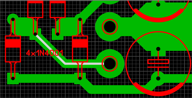
This is what these microcircuits look like in DIP packages, and their dimensions between the legs are 2.54 mm and between the rows of legs these dimensions are 7.62 mm.
Now let’s draw these microcircuits and save them as a macro, so that we don’t have to draw again in the future and we will have a ready-made macro for subsequent projects.
We launch our program and set the active layer K2, the size of the contact pad is equal to 1.3 mm, its shape is selected “Rounded vertically”, the width of the conductor is equal to 0.5 mm, and the grid pitch is set to 2.54 mm.
Now, according to the dimensions that I gave above, let’s draw our microcircuit.
Everything worked out as planned.
Then we will save our future payment. Click on the floppy disk icon and enter the file name in the field.
We have drawn the location of the legs of the microcircuit, but our microcircuit has some kind of unfinished look and looks lonely, we need to give it a neater look. We need to make a silkscreen outline.
To do this, switch the grid pitch to 0.3175, set the conductor thickness to 0.1 mm and make layer B1 active.
With this triangle we will indicate where we will have the first pin of the microcircuit.
Why did I draw it this way?
Everything is very simple, in our program by default there are five layers: layers K1, B1, K2, B2, U.
Layer K2 is the soldering side (bottom) of the components, layer B1 is the marking of the components, that is, where to put something or a silk-screen printing layer that can then be applied to the front side of the board.
Layer K1 is the top side of the board if we make the board double-sided, respectively, layer B2 is the marking or silk-screen printing layer for the top side and, accordingly, layer U is the outline of the board.
Now our microcircuit looks neater and neater.
Why do I do this? Yes, simply because I’m depressed by boards that are made haphazardly, and sometimes you quickly download some thread for the board from the network, and there are only contact pads and nothing else. We have to check each connection according to the diagram, what came from where, what should go where...
But I digress. We made our microcircuit in a DIP-14 package, now we need to save it as a macro so that later we don’t have to draw something like this, but simply take it from the library and transfer it to the board. By the way, you are unlikely to find an SL5 without macros at all. Some minimum set of standard cases is already in the macros folder. And entire sets of macro-assemblies circulate on the network.
Now hold down the left mouse button and select everything we just drew.
And all our three objects will be grouped into one
Here is the letter M on the microcircuit.
And look at our just created macro in the macro window
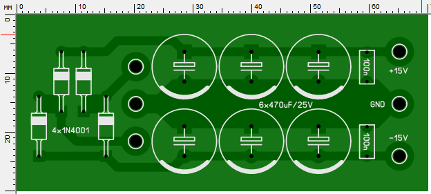
Great, but it wouldn’t hurt to decide what size our board would be. I figured out the dimensions of the parts and how they could be roughly scattered and calculated that in the end my size was 51mm by 26mm.
Switch to layer U - the milling layer or board border. At the factory, they will go through this contour with a milling cutter during manufacturing.
Select a grid pitch equal to 1 mm
An observant person will say, yeah, the starting point of the contour does not lie directly at zero and he will be absolutely right. For example, when I draw my boards, I always retreat 1 mm from the top and left. This is due to the fact that in the future the payment will be made either
using the LUT method or using a photoresist, and in the latter it is necessary that the template have negative tracks, i.e. white tracks on a dark background, and with this approach to board design, the finished template is then easier to cut out and make several copies on one sheet. And the board itself looks much more beautiful with this approach. Many people have probably downloaded boards from the network and the most funny thing happens when you open such a board and there is a drawing in the middle of a huge sheet and some kind of crosses around the edges.
Now let's change the grid pitch to 0.635 mm.
And we’ll roughly install our microcircuits
And put two contact pads at a distance of 2.54 mm
And on it we will draw the approximate radius of our capacitor; for this we need the arc tool.
So we got our capacitor, look at the diagram and see that it is connected to pins 4,5 and 1 of the microcircuit, so we’ll plug it in approximately there.
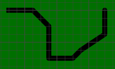
Now let’s set the width of the track to 0.8 mm and start connecting the legs of the microcircuit, we connect it very simply, first we clicked on one leg of the microcircuit with the left button of the microcircuit, then on the other, and after we brought the conductor (track) to where we wanted, click the right one, after that clicked right the path will no longer continue.
 |
Now, using a similar principle, we build parts, placing them in our board, drawing conductors between them, scratching our heads when we can’t lay a conductor somewhere, thinking, laying conductors again and in some places do not forget to change the width of the conductor, thus gradually building the board, also When laying conductors, press the spacebar on the keyboard; this button changes the bending angles of the conductor, I recommend trying this cool thing. Separately, I would like to dwell on grouping objects. Several objects can be collected into one by clicking on them with the left mouse button while holding Shift, and then click group. So, we draw, we draw, and in the end we get this:
The resulting board looks like this:
Now a little explanation on printing a mirror/non-mirror image. Usually the problem arises with LUT when, due to inexperience, you print an image in the wrong display. The problem is actually solved simply.
In all board layout programs, it is accepted that the PCB is “transparent”, so we draw the tracks as if looking through the board. It’s easier this way, in the sense that the numbering of the pins of the microcircuits turns out natural, and not mirrored, and you don’t get confused. So here it is. The bottom layer is already mirrored. We print it as is.
But the top one needs to be mirrored. So when you make a double-sided board (although I don’t recommend it, most of the boards can be placed on one side), then its top side will need to be mirrored when printing.
Now we have drawn a simple scarf, there are only a few small touches left.
Reduce the overall size of the working field and print. However, you can simply print it as is.
Let's set several copies, you never know if we mess it up:
All this is good, of course, but it wouldn’t hurt to finish the scarf itself, bring it to mind, and put it in the archive, in case it comes in handy, or needs to be sent to someone later, but we don’t even have the elements signed, what and where it is, in principle It’s possible, and so we remember everything, but the other person to whom we give it will swear for a long time, checking it against the diagram. Let's make the final touch, put the designations of the elements and their denomination.
First, let's switch to layer B1.
After we have placed all the designations of the elements, we can align them so that it looks more neat, after all these actions our scarf looks like this:
And in the field we write our value of resistor R1 according to the diagram, it is 1.5K
We wrote it, click OK and then if we move the pointer to resistor R1, its value will be displayed.
Right on the inscription, right-click and select New Board from the drop-down menu. After we answer the question in the affirmative, open the properties of the new scarf and call it TQFP-32.
Now we open the datasheet for the microcircuit that we are going to draw, for example, we will do it by looking at the datasheet from ATmega-8.
We look at the chip in the datasheet and see a square with a pancake leg on each side, well, no problem, just select another location in the top drop-down menu, namely Quadruple, and click on the SMD contact. That’s all now, looking at the datasheet, and in this window we look where to enter which parameter, in the end we fill in all the fields, and we get the following result:
Now we have a very small touch left - zoom in on the image by turning the mouse wheel away from you, switch to layer B2, and draw the outline of the microcircuit and indicate where we will have the first leg.
 |
That's all, our case for the TQFP-32 microcircuit has been created, now if you can print it out, attach the microcircuit to a piece of paper, and if it’s a little off, then slightly adjust the parameters, and then save it as a macro so that you don’t have to draw a similar case in the future.
Rendering a picture
And the last step of our lesson, I will tell you how to make a scarf from an image of a board found in a magazine or on the Internet.
To do this, let's create the following tab and call it Internet.
In order not to search for a long time to repeat, let’s go to the Internet and type “Printed circuit board” in a search engine; the search engine will throw out a bunch of links and pictures; we’ll choose something from them just like that.
After we have drawn it, let’s take our image and, using a graphic editor, remove everything that is on the left side, we basically don’t need it, and save the right side to a file with the extension .BMR. If we are scanning a scarf from some magazine, it is better to scan with a resolution of 600 dip and save it to a file.BMR After saving it in the program, go to the K2 layer and click on the TEMPLATE icon.
Click the Upload button... and select our file. After this, our screen will look like this
That's all, now we just outline this picture in detail. There are quite possible cases when the details may not fit 100% into what is drawn in the picture, this is not scary, the main thing is that there is a picture on the background layer and a set of macros with a fixed size, and this is the most important thing. The Sprint-Layout program has an excellent set of macros, and gradually, when new details are drawn, it will also be replenished with its own.
If you click on the top one, then while we hold it, our paths will become invisible, and if on the bottom, then while we hold it, our picture that was superimposed as the background will become invisible.
That’s basically all I think about the Sprint-Layout program for beginners to master it, there is already plenty of information and of course you need to remember everything what and where to click, how and what to do. And at the end of the lesson about the Sprint-Layout program, you can download the file itself with these boards, on which this program was mastered.
Happy board making!
We got acquainted with the program interface. We'll start the second part of the course by looking at what functions the program for drawing circuit boards provides.
All elements are located on the left panel.
Let's look at them.
Hotkey "Esc".
The default tool. Used to select elements on the workspace. Resetting any tool to the “Cursor” is done by clicking the right mouse button.
Hotkey "Z".
The cursor changes to a magnifying glass. Clicking on the left mouse button on the working field increases the scale of the board, and clicking on the right mouse button decreases it.
Also, with the left mouse button held down, you can select the area of the board that needs to be enlarged.
Hotkey "L".
A tool for drawing a path of a given width. The width value (in mm) is set before starting drawing in the special field below:
The button on the left opens a submenu of frequently used, so-called “favorite” track widths. You can add a new value or remove an existing one:

Note - The item to add a new value becomes active only if the current track width value is not in the list.
After setting the width, selecting the "Path" tool, you can start drawing the path directly. To do this, in the work field, select the point where the line will begin, click the left mouse button and draw the line to the point where it should end.

You can change the type of track bend by pressing the Spacebar. Five options are available:

When you press the "Space" key while holding down the "Shift" key, the search is performed in the reverse order.
During the drawing process, you can, if necessary, fix the line by clicking on the left mouse button, thereby forming the required shape of the track.
The length value is displayed for the last unfixed segments.
By holding down the "Shift" key you can temporarily make the grid step half as large, and by holding down "Ctrl" you can disable snapping the cursor to the grid.
Having fixed the last point of the track, you can finish drawing the track by clicking on the right mouse button. The track ends and the cursor is ready to draw the next track.
When you select a drawn line, it is highlighted in pink and the properties panel changes appearance, displaying the path parameters:
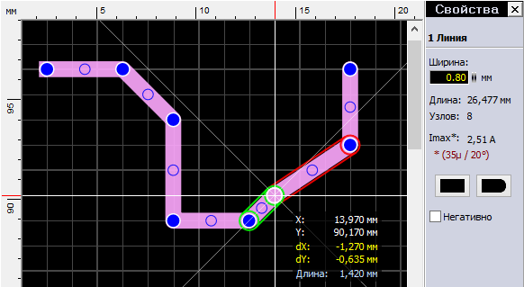
In this panel you can change the value of the line width, view its length, the number of nodes and the calculated maximum allowable current.
Note - Calculation parameters (copper layer thickness and temperature) are configured in the "I max" section of the main program settings (see).
The blue circles represent the nodes of the track. And in the middle of each track segment you can see blue circles - the so-called virtual nodes. By dragging them with the mouse cursor you can turn them into a full-fledged node. Note that during editing, one segment is highlighted in green and the other in red. Green color means the segment is horizontal, vertical or at an angle of 45°.
The ends of the tracks are round by default, but there are two buttons in the properties panel that make them rectangular (note the left end of the track).
If one trace is represented on the board by two separate tracks and their end nodes are located at the same point, then the tracks can be connected.
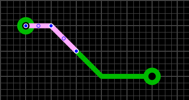

To do this, right-click on the end node and select "Connect Line" from the context menu. The track will become solid.

The "Negative" checkbox forms a cutout from the track on the Auto-ground polygon:
Contact
Hotkey "P".
A tool for creating pads for component pins. By clicking on the small triangle on the left, a contact menu opens where you can select the desired contact form:
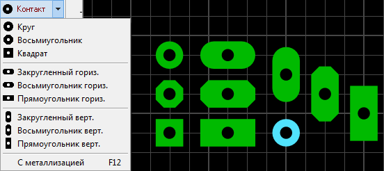
The item “With metallization” makes the contact pad on all layers of copper, and the hole metallized. In this case, the color of the contact with a metallized hole differs from those without metallization (note the round blue contact). The F12 hotkey enables/disables metallization for any selected contact.
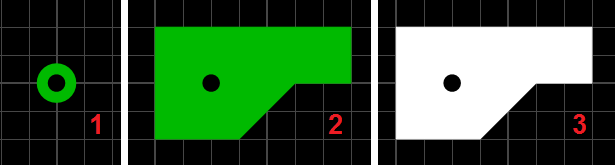
The shapes of the contact pads are not limited to this list - they can be made of any shape. To do this, you need to place a regular contact (1), and draw a pad of the desired shape around it (2). Moreover, you should not forget about the mask - you must manually open the entire contact (3) from it (see below about the mask).
Like the "Track" tool, this tool has its own settings at the bottom:
The upper field specifies the diameter of the contact pad, the lower field specifies the diameter of the hole. The button on the left opens a submenu of frequently used contact sizes. You can add a new value or remove an existing one:

Having set the required values, select the “Contact” tool and left-click the mouse to place the contact at the desired point in the working field.

The settings of any selected contact (or group of contacts) can always be changed in the properties panel:
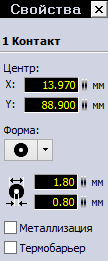
The last item with a checkmark turns on the thermal barrier at the contact. We'll look at this feature in more detail in the next part of the course.
If the contact pad does not have a warranty belt, i.e. The diameter of the hole is equal to the diameter of the contact pad, then it is displayed as follows:
SMD contact
Hotkey "S".
A tool for creating rectangular contacts for surface mount components. Settings:
On the right are fields for entering the width and height of the contact. Below them is a button for changing the values in these two fields. The button on the left opens a submenu of frequently used contact sizes.
Having specified the required dimensions and selected this tool, the contact can be placed on the working field:
For an SMD contact, the thermal barrier function is also available in the properties panel, with the only difference that it can be configured only on one layer.
Circle/Arc
Hotkey "R".
Primitives - circle, circle, arc.
We select the placement point and, holding the left mouse button, move the cursor to the side, thereby setting the diameter of the circle.

Note that the properties panel as you draw contains information about the circle being created. By releasing the left mouse button, we complete the creation of the circle. By selecting it with the "Cursor" tool, we can edit the properties of the circle in the properties panel - in particular, set the coordinates of the center, line width and diameter, as well as the angles of the start and end points if we want to turn the circle into an arc.
You can also turn a circle into an arc by dragging the cursor over the only node on the circle:

The "Fill" checkbox makes a circle out of a circle, filling the inner area, and "Negative", by analogy with a path, turns the element into a cutout on the Auto-ground polygon.
Polygon
Hotkey "F".
A tool for creating areas of any shape. Drawing occurs along a path with a given width:

Once completed, the polygon is displayed with a fill and, when selected, the nodes can be edited (same as in the path tool):
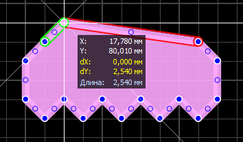
The properties panel contains some more settings:
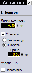
You can change the width of the contour line, see the number of nodes, make a cutout from the polygon using the Auto-earth fill (check “Negative”), and also change the type of polygon fill from solid to mesh.

The thickness of the grid lines can be left as the polygon outline, or you can set your own value.
Text
Hotkey "T".
Text label creation tool. When you select it, the settings window opens:
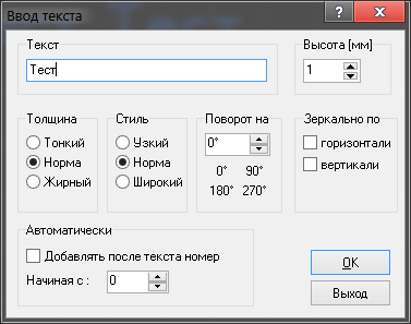
- Text- input field for the required text;
- Height- text line height;
- Thickness- three different types of text thickness;
- Style- text style;
- Turn on- rotate the text to a certain angle;
- Mirror by- reflect text vertically or horizontally;
- Automatically- additionally add a number after the text, starting from a certain value.
Three types of text thickness and three types of style give nine style options (although some are the same):

Note - By default, the minimum possible text thickness is limited to 0.15 mm. If the thickness is too small, the text height is automatically increased. This restriction can be disabled in the program settings menu (see).
Rectangle
Hotkey "Q".
Tool for creating a rectangular outline or rectangular polygon. To draw, click the left mouse button in the work field and, without releasing, move the cursor to the side, setting the shape of a rectangle.

The creation of the rectangle will be completed after the button is released.
As I already said, two types of rectangles are available - in the form of an outline from paths and with a fill.

Moreover, a rectangle in the form of an outline is nothing more than an ordinary path laid in the shape of a rectangle, and a rectangle with a fill is a polygon. Those. Once created, they can be edited as a track and a polygon, respectively.
Figure
Hotkey "N".
Tool for creating special shapes.
The first type of figure is regular polygon:

Bisector settings are available - distance from center to vertices, track width, number of vertices, rotation angle.
The "Vertex" checkbox connects opposite vertices to each other (middle picture), "Fill" - paints the interior space of the figure (right picture):

It should be noted that the result is elements consisting of tracks and a polygon. Therefore, they are edited accordingly.
The second type of figure - spiral:
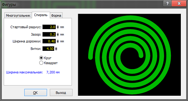
By setting the parameters, you can create a round or square spiral:
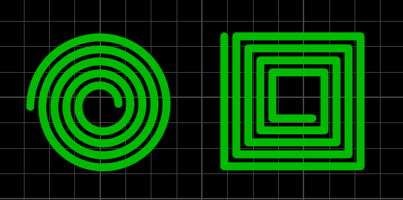
A round spiral consists of quarter circles of various diameters, and a rectangular spiral consists of a track.
The third type of figure - form:

The settings allow you to set the number of rows and columns, the type of numbering, its location, and the overall dimensions of the form. Result:

The form also consists of simpler primitives - track and text.
Mask
Hotkey "O".
Tool for working with solder mask. When using it, the board changes color:

The white color of the elements means that the area will be open from the mask. By default, only the contact pads are exposed to the mask. But left-clicking on any element of the current copper layer opens it from the mask (in the picture I opened a path from the mask in the center of the picture). Pressing it back again closes it.
Connections
Hotkey "C".
The tool allows you to establish a virtual connection that is not broken when moving or rotating components between any contacts on the board.
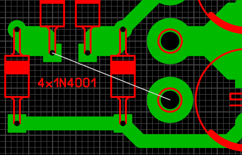
To delete a link, you need to left-click on it with the Link tool active.
Highway
Hotkey "A".
A primitive autorouter. Allows you to trace placed "Connections".
To do this, set the routing parameters (track width and gap) and hover the cursor over the connection (it will be highlighted) and click the left mouse button. If it is possible to lay a route with the specified parameters, then it will be laid:
In this case, the automatically laid route will be displayed with a gray line in the center of the track. This makes it possible to distinguish them from manually laid routes.
Clicking the left mouse button again with the Route tool active on the automatically routed route deletes it and returns the contact link.
Control
Hotkey "X".
The tool allows you to see the entire routed circuit by highlighting it:

Note - in the first part of the course I described setting the type of this backlight: flashing/non-blinking Test mode.
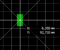
Meter
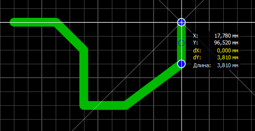
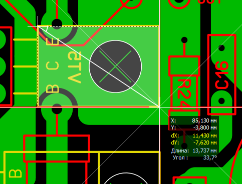
Hotkey "M".
By holding down the left mouse button, a rectangular area is selected, and a special window displays the current coordinates of the cursor, changes in coordinates along two axes and the distance between the start and end points of the selection, and the diagonal angle of the selection rectangle.
Photoview
Hotkey "V".
A handy tool that allows you to see what the board will look like after manufacturing:


The Top/Bottom switch changes which side of the board is displayed.
Note - The bottom layer is mirrored when displayed compared to the display when tracing. The PhotoView tool works in the same way as if you were twirling a finished board in your hands.
The "With components" checkbox enables the display of the marking layer, and the "Translucent" checkbox makes the board translucent - the bottom layer is visible through it:
Two drop-down menus - “Board” and “Solder mask” change the color of the mask and the color of the contacts not covered by the mask:

Note - The "---" item displays the contacts as covered with a mask.
Macros
A macro is a saved area boards, ready for further reuse. In Sprint Layout A library of component footprints is organized in the form of macros.
After starting the program, by default the macro panel is open on the right. Opening/closing this panel is controlled by a button on the toolbar on the right side of the window:
This library is currently empty.
To connect the downloaded set of macros, just unpack it and place it in the folder specified in the SL6 settings (see):

After this, the program, having scanned this folder during the next launch, will display macros in the panel:

To delete a macro from the library, just select it in the library tree and click on the trash can icon next to the save button.
To edit a macro, you need to drag it onto the work field, make the necessary changes and, having selected the necessary elements, click on the “Save” button and save it as a new macro, giving it a name (or replace the existing one).
IPC-7251 and IPC-7351
I would like to say a few words about naming your macros. There are foreign standards IPC-7251 and IPC-7351, which determine the sizes of contact pads and types of footprints for various standard cases. But in our case, we will need recommendations on naming the footprints from there.
Let's look at the example of a 100 nF capacitor of the B32922 series from EPCOS:

According to the IPC-7251 standard, the name of its footprint will be formed as follows:
CAPRR + Lead-to-pin distance + W Lead thickness+ L Body length + T Case thickness+ H Case height
Therefore, according to the datasheet we have:
CAPRR_1500_ W80_ L1800_ T500_ H1050
CAPRR– Capacitor (CAP), non-polar, radial (R), rectangular (R)
1500
– Pin spacing = 15.00mm
W80– Lead thickness = 0.80mm
L1800– Case length = 18.00mm
T500– Case thickness = 5.00mm
The following parameter is optional - for Sprint Layout it has no meaning:
H1050– Case height = 10.50mm
Thus, this type of naming, after getting used to it, will allow you to find out information about the footprint by the name of the macro and avoid confusion in the library.
I have attached excerpts from the standards to the article:
- Footprint Naming Convention. Surface Mount - for SMD components.
- Footprint Naming Convention. Through-hole - for output components.
Creating Macros
As an illustrative example, we will select a circuit for which we will create a library of macros. Let this be a simple tone control on the TDA1524A chip:

Let's carefully look at the diagram and make a list of components for which we will need macros:
- Chip TDA1524A.
- Fixed resistor with a power of 0.25 W.
- Variable resistor.
- Electrolytic capacitors.
- Film capacitors.
- Connectors for connecting power, as well as for connecting a signal source and load.
- Miniature switch.
The process of creating a macro consists of several steps:
- Arrangement of contacts.
- Drawing graphics for the marking layer.
- Saving the macro in a separate file on disk.
In the video below I will show you the process of creating macros for elements of the selected diagram in two ways.
Once upon a time, creating a printed circuit board (PCB) for an electronic device was just an add-on, a supporting technology to improve quality and repeatability in mass production of electronics. But this was at the dawn of the development of electronics. Now the creation of software is a whole separate branch of technical art.
As Wikipedia says, PP is:
A dielectric plate on the surface and/or in the volume of which electrically conductive circuits of an electronic circuit are formed. A printed circuit board is designed to electrically and mechanically connect various electronic components. Electronic components on a printed circuit board are connected by their terminals to elements of a conductive pattern, usually by soldering.
Today, radio amateurs have access to factory production to order their printed circuit boards. It is enough to prepare the necessary files with a printed circuit board design and additional information about holes, etc., send it to production, pay and receive ready-made factory-quality PCBs with silk-screen printing, solder mask, precisely drilled holes, etc. Or you can make PP the old fashioned way at home using LUT and a cheap etching solution.
But before you make a PP, you need to draw it somehow. Currently, there are dozens of programs for these purposes. They can be used to design both single-layer and multi-layer printed circuit boards. In RuNet, the Sprint Layout program is most widespread among radio amateurs. You can draw PP in it as in a graphics editor. Only your own specialized set of drawing tools. This program is simple, convenient and a good place to start your acquaintance with PCB design in CAD.
It's not my goal to create a complete guide. There are a huge number of SL tutorials on the Internet, so I will try to give a concise description so that you can quickly get down to business - drawing a printed circuit board, so I will try to talk about some useful SL functions that are really needed when creating a PCB.
General view and working area
The program itself looks like a regular Windows application: at the top there is a strip with the program menu (file, actions, board, functions, service, options, help). On the left is a panel with tools that are used when drawing a printed circuit board. On the right is a window that displays the properties of the working field, a specific track, a specific group of tracks, etc. Those. If you select an object on the PP, its properties will be displayed in the window on the right. A little further to the right of the “Properties” window is the “Macros” window. Macros are a convenient tool for grouping and reusing previously drawn parts or parts of a board. I will dwell on them in more detail, since they save incredible time and reduce the number of errors on the board.
Working field
The black mesh field is the working field. This is where you will place contact pads, holes for radio components and draw tracks between them. The field also has some properties. The obvious ones are length and width. The field size determines the maximum size of the PP. In this case, the width and length are specified in millimeters. This is an important clarification, since the grid cell size is set by default not in millimeters, but in mil (i.e., not metric, but inch units):

This strange measure of length came to us from England and is equal to 1/1000 of an inch:
1 mil = 1 ⁄ 1000 inch = 0.0254 mm = 25.4 microns
Mil is widely used in electronics, but in Sprint Layout you can configure the grid to be displayed in mm. Install it the way that is most convenient for you. Mil is a smaller measure and therefore allows you to more accurately position the elements of the printed circuit board on the working field.
Sprint Layout Toolbar
Cursor (Esc) is a common tool that is used to select an element on the PP: a hole or part of a track.
Scale (Z) -- used to increase/decrease the size of the printed circuit board pattern. It is convenient when there are many thin paths and you need to highlight one among them.
Track(L)-- used to draw a conductive path. This tool has several operating modes. More on them later.
Contact(P)-- the tool is designed for drawing vias. You can select the shape of the hole, and also set the radius of the hole itself and the radius of the foil around it.
SMD contact (S) - for designing PCBs using SMD components. Draws contact pads of the required sizes.
Circle/Arc (R) -- to draw a conductor in the shape of a circle or arc. It can be convenient in some cases.
Square (Q), Polygon (F) , Special forms (N) -- tools for creating sites and areas of a certain type.
Text(T)-- for writing text. You can set how the text will be displayed on the board: normally or mirrored. This helps to display correctly on the board, for example when using LUT.
Mask (O) -- for working with solder mask. By default, when you turn on this tool, the entire board except the pads is “covered” with a solder mask. You can arbitrarily open/close any contact or track with a solder mask by clicking on it with the left mouse button.
Jumpers (C) is a virtual connection that is preserved during any manipulations with the contact tracks between which it is installed. When printing, the jumpers are not displayed in any way, but they are used for auto-routing.
Highway (A) is the simplest autorouter. Allows you to lay contact paths between contacts using arranged connections. In order to distinguish automatically laid paths from manually laid ones, SL draws a gray line in the middle along such a path.
Test (X) is the simplest control tool. It can be used to highlight one specific track in a layer. Convenient for checking the correct layout of tracks.
Meter (M) is a convenient tool for measuring distances on a board drawing. The meter shows: cursor coordinates, changes in cursor coordinates in X and Y, the distance between the start and end points and the diagonal inclination angle of the rectangle constructed from the start and end points of the meter.
Photo view (V) -- shows approximately what your board should look like after industrial manufacturing.
SL allows you to draw multilayer PCBs. For home purposes, you are unlikely to go beyond a 2-layer board. But if you order from production, then Sprint Layout has the necessary capabilities for rendering a board with several layers. There are seven in total: two outer copper layers (top and bottom), two silkscreen layers for the outer layers, two inner layers, and one non-printed layer for drawing the outline of the board.

Working with layers is similar to working with layers in Photoshop or GIMP (If you haven’t used gimp, I recommend it. It’s like Photoshop, only free): you can place tracks in different layers, turn layers on and off, etc. Switching the working layer and controlling visibility is done at the bottom of the working field using this control:
Each layer in SL has its own purpose:
- M1- upper layer
- K1- marking of elements of the top layer
- IN 1- inner layer
- AT 2- another inner layer
- M2- bottom layer
- K2- marking of elements of the lower layer
- ABOUT- layer for drawing board outlines
When creating your board, you should remember that the text and elements in the M2 layer must be reflected. Usually SL automatically makes the text reflected, but you should still check from time to time.
When working in SL, only one layer is always active. It is on this layer that all contact pads and tracks will be placed. While working with this layer, all other layers are considered inactive - tracks and contacts on them cannot be changed.
Macros and element libraries
Each electronic component has its own dimensions, its own number of pins, etc. You won’t draw them by eye every time, especially since there are macros and entire libraries of macros for this with already verified and prepared components.
Macros are a small piece of PCB board that you can use multiple times. In Sprint Layout, you can turn anything into a macro and then reuse it over and over again in other projects. Very useful and convenient.
Macros can be combined into libraries. At the same time, the library is just an ordinary folder in which a bunch of macros are piled up, which are interconnected by some kind of logic. For example, these are smd resistors or Soviet operational amplifiers, etc. Macros and libraries are most often located in the root folder of the SprintLayout/MAKROS/ program
The process of creating a macro is very simple:
- We arrange contacts
- In the marking layer we draw a graphic designation of the component
- Save the macro
Little tricks when working with Sprint Layout
#1 hotkeys
Although clicking on icons with the mouse is quite convenient, SL has the ability to control almost everything from the keyboard, which increases the speed of work.
| Arrows Up, Down, Left, Right | Allows you to move components across the working field by 1 grid step in 1 click. If you also hold down Ctrl, the step will be 1/100 mm |
| Ctrl | Unsnaps the snap to the grid. This allows, for example, to reduce the movement step |
| F1-F4 | Selecting a layer. Each key activates the corresponding layer |
| F5-F8 | Make layer visible/invisible |
| Delete | Delete something on the workspace |
| Space | Allows you to switch the bend of the conductor. In total, SL has 5 types of bending of the conductive track. |
| Ctrl+C | Copy selection |
| Ctrl+Y | Redo undone action |
| Ctrl+Z | Cancel action |
| Ctrl+X | Cut selection. Will be buffered |
| Ctrl+V | Paste from clipboard |
| Ctrl+D | Duplicate selection |
| Ctrl+A | Select all components in the field |
| Ctrl+R | Rotate selection |
| Ctrl+H | Flip selection horizontally |
| Ctrl+T | Flip selection vertically |
| Ctrl+G | Grouping selected components into a group |
| Ctrl+U | Breaking a group down into its constituent components |
| Ctrl+W | Move selection to the back of the board |
No. 2 Fast grid spacing switching
I wrote above that the grid step can be selected, but I did not say that using keys 1 to 9 you can quickly change the grid step. They are easily configured via "hot keys" in the grid settings menu.
No. 3 Cascade installation of elements
In the "Actions" menu there is an interesting function "Cascade/Cascade in a circle". It allows you to arrange contacts or components in a cascade: along a given radius or in the form of a matrix. It is very convenient when you need to create many identical elements or pads located in a circle or in a grid.
No. 4 Filling empty space with copper
For various reasons, it is sometimes necessary to cover the empty space on the board with copper so that it does not short circuit with the traces of the board. In Sprint Layout, there is a button at the bottom of the work field for these purposes:
No. 5 Several boards on one sheet
There are several ways to get several identical boards on one sheet. First, you can simply select the entire board and copy it as many times as needed. Secondly, you can turn such a board into a macro and simply use the macro to copy the board. Very convenient if you need to make a panel from circuit boards. True, this is not necessary to transfer to production - they will be able to make such panels themselves. The only exception is the case when you need to place several different boards in one file.
No. 6 Installation of reference marks
If you suddenly plan to not only order a PCB in production, but also perform automatic installation of SMD components, then you should familiarize yourself with the reference points and how to install them.
In general, reference points are special marks on the PCB that allow assembly robots to correctly recognize the position and pattern of the printed circuit board during the installation process.
Commonly accepted reference marks look like this:

Using fiducial marks, you can help the mounting equipment to accurately determine the position of the board itself on the panel (if several identical boards are located on one panel), and specific elements on the board. Conventionally, all reference marks can be divided into 4 groups:
- Common PCB Fiducial Marks
- Local reference marks of individual elements
- PCB Panel Fiducial Marks
Sprint Layout 6 has the ability to create fiducial marks. To do this, draw a reference mark on the copper layer, then go to the mask editing mode ("O" key) and remove the mask over the drawn circle. Next, when exporting Gerber files, you should set the gap for the solder mask to the required size (This will not affect the gap between the mask and the contacts, since such a gap is adjusted separately, but it will affect the gaps between other PCB elements forced open from the mask).
No. 7 How to change the type of bend of the track
In order to change the bend of the track in SL, you just need to press the space bar (selecting the track drawing tool - L in front of these). The following types of bends are available for drawing:

I’ll finish here, since the Sprint Layout program is very simple (but at the same time very convenient and useful) and you will get much more pleasure by experimenting on your own. Take action!
/blog/sprint-layout-dlya-nachinayuschih/ Learn to draw professional PCBs yourself with Sprint Layout. This is the most popular program for creating PP among radio amateurs of all ages and skills. 2016-12-20 2017-02-04 sprint layout, layout 6.0, sprint layout rus, sprint layout 7.0Great radio amateur and program designer
There is no fundamental difference between creating a board and creating a macro. In this case, the same copper layers (M1, M2) are used for contact pads and conductors and silk-screen printing layers (K1, K2) for drawing projection lines of the component body. The application of the body projection is carried out using the simplest graphic elements (line, circle, etc.) in a silk-screen printing layer.
Example:
You need to create a macro for a 14-pin DIP package.
(This is just an example. It is quite natural that such a corpus already exists in the library.)
14 contact pads are applied to the M2 layer (bottom side) along a given grid (the grid pitch corresponds to the pin pitch). To identify the first pin, its pad can be made square.
Now you should make layer K1 active (silkscreen, top) and draw the outline of the body using the graphics commands. Additionally, you can mark a cutout on the body for better visualization.
So, the macro is almost ready.
Select a point on the working field with the cursor, press the left mouse button and, while holding it, mark the selection area. In this case, you should ensure that only those elements from which the macro is built fall into the selected area.

The selected elements will turn pink.

3. Saving a macro
To save the macro, selectSave as macro.. . on the menu File.
The same command is executed when you click the save button on the library panel.
This will open a dialog box. The save directory in it corresponds to the current library section. If you want to save the macro in another section, you must select the section accordingly.
The macro must be given a valid name. Macro file extension".lmk" (assigned by default to all macros) will be added automatically.
After saving the macro, it will be added to the selected library section.